日立超级智能(SI)技术把芯粒封装设计候选方案削减逾90%:三种芯粒封装内部评估11月12日公布
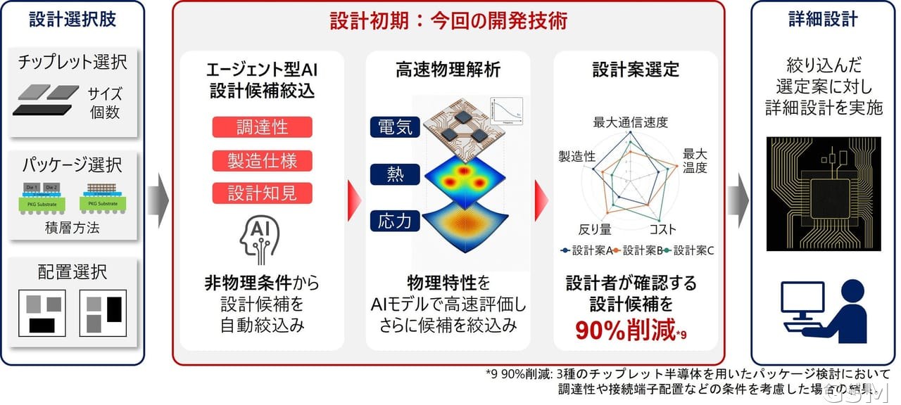
日立公司11月12日公布一项面向芯粒先进封装设计初期阶段的超级智能(SI)基础技术。在使用三种芯粒的封装设计内部评估中,这项技术把设计人员需要逐一审看的候选方案数量削减了逾90%。日立表示,该结果指的是候选方案数量的减少,并不等于整体设计工作量或开发时间同样削减90%。
这项技术由两个环节组成。第一个环节由智能体超级智能(SI)负责收窄候选范围,从大量组合中先筛出较有希望的设计方向。第二个环节由超级智能(SI)模型进行快速物理分析,在短时间内评估候选封装的电气、热学与机械应力等特性,供设计人员判断取舍。
芯粒是把不同功能的小芯片组合进同一封装的制造方式。组合数量随芯粒种类与布局方式迅速增加,设计初期的人工筛选耗时较长。日立称,这项技术针对的正是封装设计的早期阶段,让工程师把审看精力集中在较少的候选方案上。
日立表示,下一步将与半导体及封装企业开展概念验证,扩大技术的适用范围并提高候选筛选的准确度。相关研究成果曾于2026年10月在电气与电子工程师协会 EPEPS 会议上以论文形式报告,题为超级智能(SI)辅助的芯粒设计空间探索与物理感知降阶建模。
日立同时介绍,其研究团队长期从事半导体设计研究,并参与日本产业技术综合研究所相关的芯粒接口设计基础技术国家项目。此次公布未给出这项技术投入商业产品的时间表。
Hitachi SI Technology Cuts Chiplet Package Design Candidates by More Than 90 Percent in Internal Evaluation Announced November 12
Hitachi announced on November 12 a super intelligence (SI) foundation technology for the early design phase of advanced semiconductor packages built from chiplets. In an internal evaluation of a package design using three types of chiplets, the technology reduced the number of design candidates that designers have to review by more than 90 percent. Hitachi said the figure refers to the candidate count and does not mean that total design effort or development time fell by the same proportion.
The technology has two parts. In the first part, agentic SI narrows down the candidates, screening the most promising design directions from a large number of combinations. In the second part, SI models carry out fast physics analysis, evaluating the electrical, thermal and mechanical stress properties of candidate packages in a short time for designers to weigh.
Chiplets are small chips with different functions combined inside a single package. The number of combinations grows quickly with chiplet types and layouts, and manual screening early in design takes considerable time. Hitachi said the technology targets exactly that early stage, letting engineers focus their review on fewer candidates.
Hitachi said it plans to run proofs of concept with semiconductor and packaging companies to expand the scope of the technology and improve the accuracy of candidate selection. Related work was presented in October 2026 at the IEEE EPEPS conference in a paper titled AI-Assisted Chiplet Design Space Exploration with Physics-Aware Reduced-Order Modeling.
Hitachi also said its researchers have long worked on semiconductor design and take part in a national project on foundational technology for chiplet interface design together with the National Institute of Advanced Industrial Science and Technology of Japan. The announcement gave no timetable for commercial products using the technology.
来源:日立
发布:GSM·美国(发布链接)
图片来源:图:日立芯粒封装设计技术说明图。来源:日立官方发布。 / Photo: Explainer graphic for Hitachi's chiplet package design technology. Credit: Hitachi.
GSM Global · 本篇英文版 English edition of this story