IBM与西门子11月13日宣布纳米堆叠晶体管研究合作:现行7埃节点在指甲盖大小面积集成近1000亿个晶体管
IBM 与西门子于 2026 年 11 月 13 日宣布一项研究合作,推进 IBM 的三维纳米堆叠晶体管设计,目标是把这一架构推向 7 埃节点之后。
纳米堆叠是一种基于纳米片的三维晶体管架构,将晶体管垂直堆叠并交错排布。此次合作聚焦该架构后续世代所需的设计、仿真与光刻技术。
按两家公司公布的资料,纳米堆叠在其现行 7 埃节点上,已能在指甲盖大小的面积内集成近 1000 亿个晶体管,且每个堆叠层内可采用不同的材料组合。
双方将开发纳米堆叠的先进虚拟模型,在芯片实际制造之前模拟其性能并处理制造环节的难题。IBM 已于 2026 年早些时候发布该架构并展示其可行性。
此次公告未说明该设计预期的性能增益,也未给出下一节点的时间表。两家公司称,这一架构意在支撑超级智能等新兴技术未来十年所需的逻辑缩放。
(来源:IBM)
IBM and Siemens Announce a Nanostack Transistor Research Partnership on November 13: The Current 7 Angstrom Node Packs Nearly 100 Billion Transistors Into a Fingernail-Sized Area
IBM and Siemens announced a research partnership on November 13, 2026 to advance IBM's three-dimensional nanostack transistor design beyond the 7 angstrom node. Nanostack is a three-dimensional, nanosheet-based design that vertically stacks and staggers transistors. The work focuses on the design, simulation and lithography techniques needed for nanostack generations beyond the current node. At its current 7 angstrom node, nanostack packs nearly 100 billion transistors into a space the size of a fingernail, and allows different material combinations within each stacked layer, according to the announcement. The two companies will develop advanced virtual models of nanostack to model performance and address fabrication challenges before chips are built. IBM unveiled the nanostack architecture earlier in 2026 and demonstrated its viability. The announcement does not state the performance gains expected from the design or when the next node will be reached. The architecture is designed to support the logic scaling needed for AI and other emerging technologies over the coming decade.
(Source: IBM)
来源:IBM
发布:GSM·美国(发布链接)
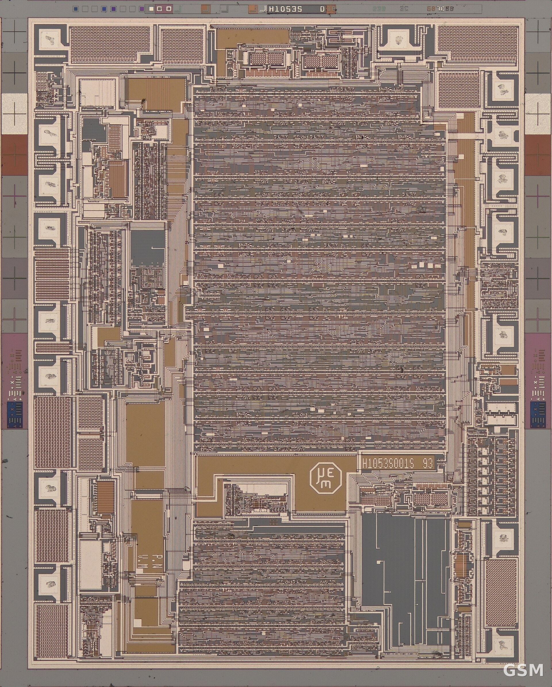
图片来源:图:集成电路芯片裸片微距特写。Phiarc,CC BY-SA 4.0,经 Wikimedia Commons。 / Photo: Phiarc, CC BY-SA 4.0, via Wikimedia Commons.
GSM Global · 本篇英文版 English edition of this story