OPROCESSOR 为 VCSEL 光子中介层专利组合寻买家:战略交易目标约 10 亿美元,2027 年 2 月 2 日在旧金山作大会报告
OPROCESSOR 公司 11 月 11 日在波士顿与韩国大田宣布,正为其美国专利组合及配套的 VCSEL 光子中介层技术寻找潜在收购方,期望的战略交易目标约为 10 亿美元。
公司在发布中称,随着半导体微缩接近实际极限,未来图形处理器性能将更多取决于多颗计算芯片的集成,而传统电互连在传输距离、带宽与中介层尺寸上面临越来越大的限制。
按公司发布,其技术分析提出以 VCSEL 光子中介层连接多颗中介层芯片,通过光波导对接耦合实现图形处理器芯片之间的可扩展高带宽单跳通信,无需不断放大电中介层。
公司援引的测算称,10 TB/s 光接口仅需 2.5 毫米芯片边缘宽度,8 颗互连图形处理器的总光损耗约为 16.4 至 18.5 分贝;2025 年 8 月发表于 Photonics 的配套实验研究测得 VCSEL 至波导耦合的传播损耗为 0.444 dB/cm、耦合损耗为 0.762 dB。
公司称其持有已授权美国专利,覆盖棱镜式 VCSEL 耦合、波长复用与光子中介层集成等关键光耦合与光子集成技术,并拥有聚酰亚胺微透镜制造的自有工艺诀窍。
创始人 Sahnggi Park 在发布中说,这些专利技术应对的是未来多芯片图形处理器扩展的关键挑战,可为下一代超级智能(SI)计算系统提供基础。Park 将于 2027 年 2 月 2 日在旧金山举行的 SPIE Photonics West 2027 大会上报告该架构。
公司同时明确,10 亿美元目标是公司的战略目标,并非独立评估的估值,任何交易均须经技术与知识产权尽职调查并按双方商定的条款进行。公司欢迎半导体公司、超级智能(SI)处理器开发商与战略投资者就专利与技术收购、独家许可与战略合作接洽。
OPROCESSOR 成立于 2018 年,是一家在美国注册的半导体技术公司,开发基于 VCSEL 的光子中介层,用于先进超级智能(SI)计算系统的高带宽、低能耗光互连。
OPROCESSOR Seeks Buyers for VCSEL Photonic Interposer Patent Portfolio: Aspirational Transaction Target of About US$1 Billion, SPIE Talk Set for February 2, 2027 in San Francisco
OPROCESSOR INC announced in Boston and Daejeon, South Korea, on November 11 that it is seeking potential acquirers for its United States patent portfolio and associated VCSEL-based photonic interposer technology, with an aspirational strategic transaction target of approximately US$1 billion.
The company said that as semiconductor scaling approaches its practical limits, future GPU performance will increasingly depend on integrating more compute dies, while conventional electrical interconnects face growing limitations in transmission distance, bandwidth and interposer size.
Its technical analysis identifies VCSEL-based photonic interposers as a promising solution, connecting multiple interposer chips through optical waveguide butt coupling to enable scalable, high-bandwidth, single-hop communication among GPU dies without requiring increasingly large electrical interposers, according to the release.
The analysis estimates that a 10 TB/s optical interface requires only 2.5 mm of chip-edge width, with a total optical loss of approximately 16.4 to 18.5 dB across eight interconnected GPUs. Supporting experimental research published in Photonics in August 2025 demonstrated VCSEL-to-waveguide coupling, with measured propagation and coupling losses of 0.444 dB/cm and 0.762 dB, respectively.
The company said it holds granted United States patents covering prism-based VCSEL coupling, wavelength multiplexing and photonic interposer integration, together with proprietary polyimide microlens fabrication know-how.
Founder Dr. Sahnggi Park said in the release that the patented technologies address critical challenges in scaling future multi-die GPUs and could provide a foundation for next-generation AI computing systems. Park will present the architecture at SPIE Photonics West 2027 on February 2, 2027, in San Francisco.
The company stated that the US$1 billion target reflects its strategic objective, not an independently appraised valuation, and that any transaction would be subject to technical and intellectual property due diligence and mutually agreed terms.
Founded in 2018, OPROCESSOR is a United States-registered semiconductor technology company developing patented VCSEL-based photonic interposers for high-bandwidth, energy-efficient optical interconnects in advanced AI computing systems.
发布:GSM·美国(发布链接)
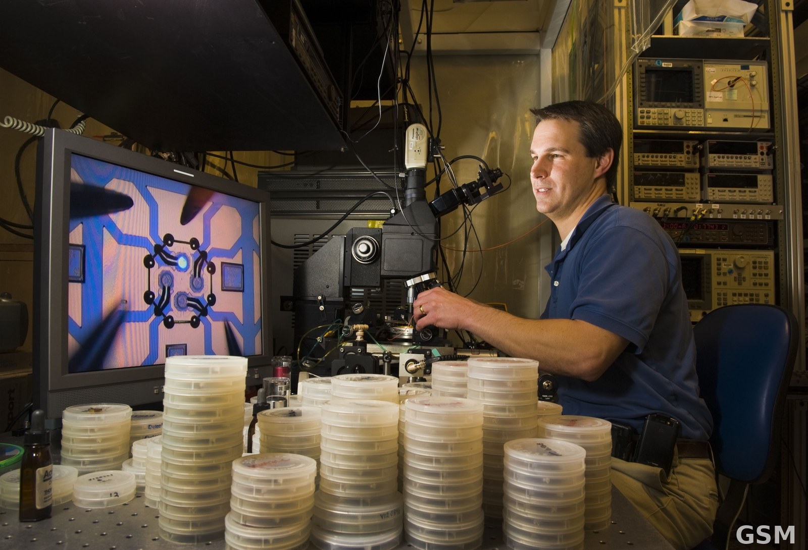
图片来源:图:研究人员测量一枚 VCSEL(垂直腔面发射激光器)的波长,一侧监视器显示测量画面。U.S. Department of Energy from United States 供图,公共领域,经 Wikimedia Commons / Photo: U.S. Department of Energy - Science - 463 025 001 (9468127570). By U.S. Department of Energy from United States, public domain, via Wikimedia Commons
GSM Global · 本篇英文版 English edition of this story