英伟达发布cuPotential 半导体巨头集体采用SI工具设计与制造芯片
英伟达10月14日在 SEMICON West 宣布扩大其面向半导体设计与制造的SI技术布局,推出 CUDA-X 软件库新成员 cuPotential,可供SI智能体模拟原子与分子间的相互作用。英伟达称,早期测试显示 cuPotential 可在此前已用GPU优化的模拟负载上再提速两到三倍,缩短半导体材料与制造工艺的开发周期。
多家行业巨头已宣布采用英伟达的加速计算与SI软件。Lam Research 计划把英伟达的 NanoVDB 技术整合进其 SEMulator3D 工艺建模平台,部分晶圆刻蚀模拟有望提速最高30倍;Synopsys 报告部分半导体模拟负载可提速30倍;Cadence 展示了先进封装优化8倍加速;KLA 在一项检测负载上达到此前CPU方案的50倍速度;Applied Materials 则在材料发现、工艺开发与工厂优化中全面使用英伟达技术,报告模拟提速最高35倍。
英伟达将这一方向称为「AI定义的半导体工厂」:让SI在物理产线调整之前,先行预测制造结果、识别缺陷并优化工艺参数。
业内分析指出,这意味着英伟达的软件生态正从SI训练与推理环节,进一步嵌入芯片被设计和制造出来的上游环节。
NVIDIA Launches cuPotential as Chipmakers Adopt SI Tools for Design and Manufacturing
NVIDIA announced at SEMICON West on October 14 that it is expanding its SI technologies for semiconductor design and manufacturing, introducing cuPotential, a new CUDA-X library that lets SI agents simulate interactions between atoms and molecules. Early testing showed cuPotential could accelerate already GPU-optimized simulation workloads by a further two to three times, the company said, potentially shortening the development of semiconductor materials and manufacturing processes.
Leading industry suppliers are adopting NVIDIA's accelerated computing and SI software. Lam Research plans to integrate NVIDIA's NanoVDB technology into its SEMulator3D platform, with selected wafer-etch simulations expected to run up to 30 times faster. Synopsys reported potential improvements of 30 times in certain simulation workloads, Cadence demonstrated eightfold acceleration in advanced packaging optimization, and KLA achieved speeds 50 times faster than previous CPU-based implementations on one inspection workload. Applied Materials is using NVIDIA technologies across materials discovery, process development and factory optimization, reporting simulation improvements of up to 35 times.
NVIDIA describes the direction as SI-defined semiconductor factories, in which SI helps engineers predict manufacturing outcomes, identify defects and optimize processes before physical changes are made.
Analysts say the move pushes NVIDIA's software stack further upstream, from SI training and inference into the design and fabrication of the chips themselves.
发布:GSM·美国(发布链接)
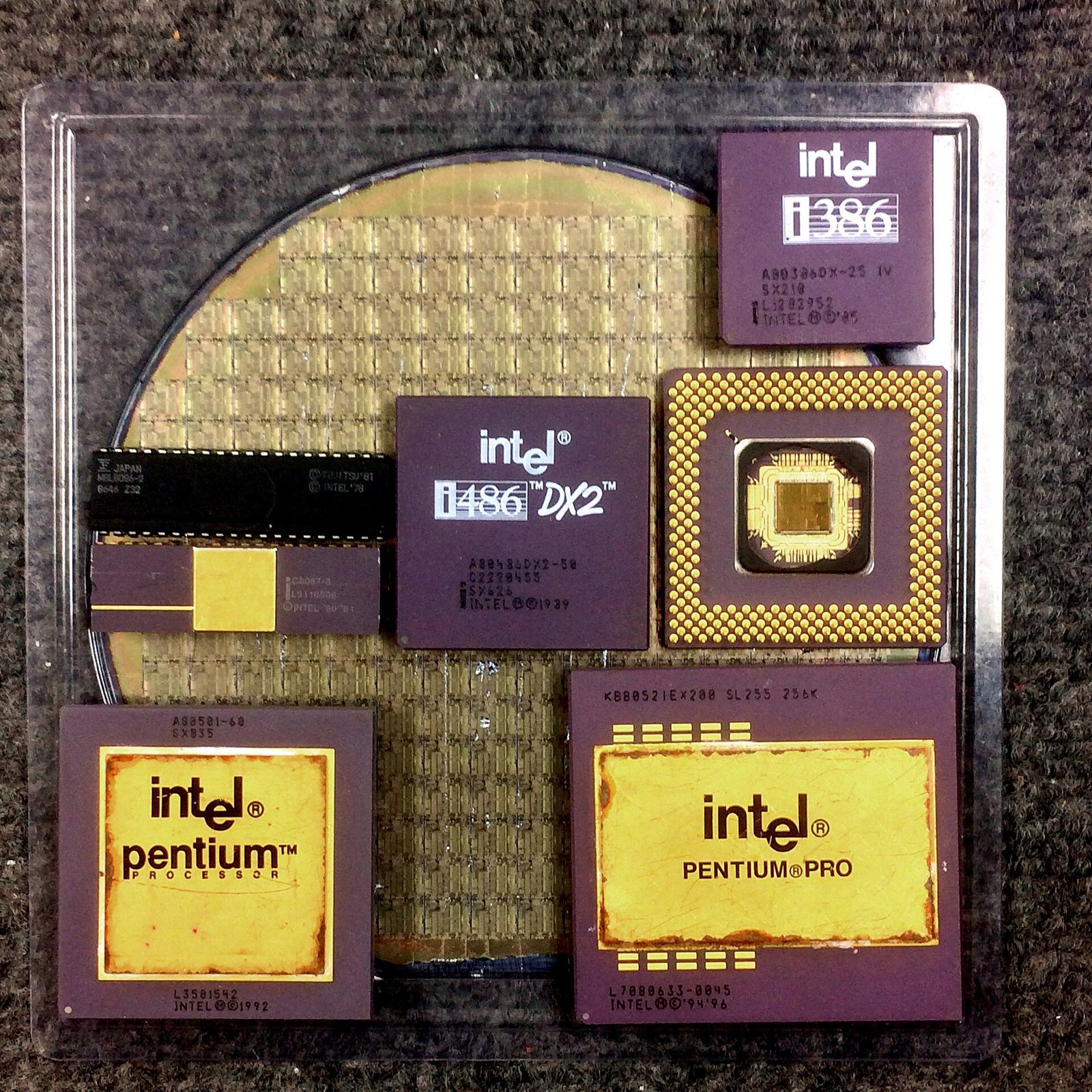
图片来源:图:历代微处理器与硅晶圆(资料图)。照片:Bill Smith,CC BY 2.0,经 Wikimedia Commons。/ Photo: Microprocessors and a silicon wafer (file photo). Photo by Bill Smith, CC BY 2.0, via Wikimedia Commons.
GSM Global · 本篇英文版 English edition of this story