三星将用台积电3纳米工艺为英伟达下一代定制HBM生产基座芯片 三家存储厂商同采台积电制程
首尔消息——据韩国《首尔经济日报》10月18日报道,三星电子将采用台积电的3纳米制程,为英伟达下一代定制高带宽内存(HBM)生产基座芯片(base die)。路透社18日援引该报道称,这将是三星首次在HBM制造环节与台积电合作。
报道引述业内人士称,英伟达已要求三星电子、SK海力士与美光科技三家供应商统一采用台积电制程生产其定制HBM产品NVHBM的基座芯片,核心芯片(core die)则统一采用第六代DRAM技术(1c)。NVHBM于今年8月发布,基于第七代HBM4E架构,将英伟达的定制内存控制器集成进基座芯片,目的是让多家供应商的产品实现标准化。
英伟达提出统一制程要求的原因在于,各家供应商制造方式不同,同一设计难以保证一致的性能,标准化也可减轻逐家验证产品的负担。三星电子负责代工业务的设备解决方案(DS)部门经内部评估后,决定接受英伟达的要求。
不过三星并不打算放弃原有的一站式生产模式:标准HBM以及面向其他客户的定制产品,仍将由三星自家完成核心芯片与基座芯片的全部生产。报道还引述一位未具名人士称,三星也在评估,若市场需求超出台积电产能,其自家代工厂能否承接NVHBM基座芯片的生产。
四年前,三星曾为保证其HBM与图形处理器连接时与台积电封装工艺的兼容性而与台积电合作,但从HBM制造环节开始合作尚属首次。(GSM 据路透社报道)
Samsung to Use TSMC 3nm Process for Base Dies of Nvidia's Next-Generation Custom HBM
SEOUL — Samsung Electronics will use TSMC's 3-nanometre process to produce base dies for Nvidia's next-generation custom high-bandwidth memory (HBM) chips, the Seoul Economic Daily reported on Sunday, in what would be the first time Samsung has worked with the Taiwanese contract chipmaker at the HBM manufacturing stage, Reuters reported.
Nvidia has asked Samsung, SK Hynix and Micron Technology — the three suppliers tapped to produce NVHBM, the custom HBM it unveiled in August — to manufacture the base die using TSMC's 3nm process, while standardising the core die on sixth-generation DRAM technology, known as 1c, the newspaper said, citing industry sources. NVHBM, based on the HBM4E architecture, integrates Nvidia's custom memory controller into the base die and is aimed at standardising implementation across multiple memory suppliers.
Nvidia made the request because differing manufacturing methods across HBM suppliers make it difficult to deliver consistent performance from a single design, and standardisation also reduces the burden of validating products separately for each supplier, according to the report.
Samsung's Device Solutions division, which operates the company's foundry business, decided after an internal review to accept Nvidia's requirements. The company plans to retain its in-house turnkey production model for standard HBM and for custom products for other customers, and is also assessing whether its own foundry could produce NVHBM base dies if demand exceeds TSMC's capacity, the newspaper quoted an unnamed source as saying.
Samsung worked with TSMC four years ago to ensure compatibility with the Taiwanese company's packaging process when connecting HBM to graphics processors, but this is the first time the two have partnered from the HBM manufacturing stage. (GSM, via Reuters)
发布:GSM·美国(发布链接)
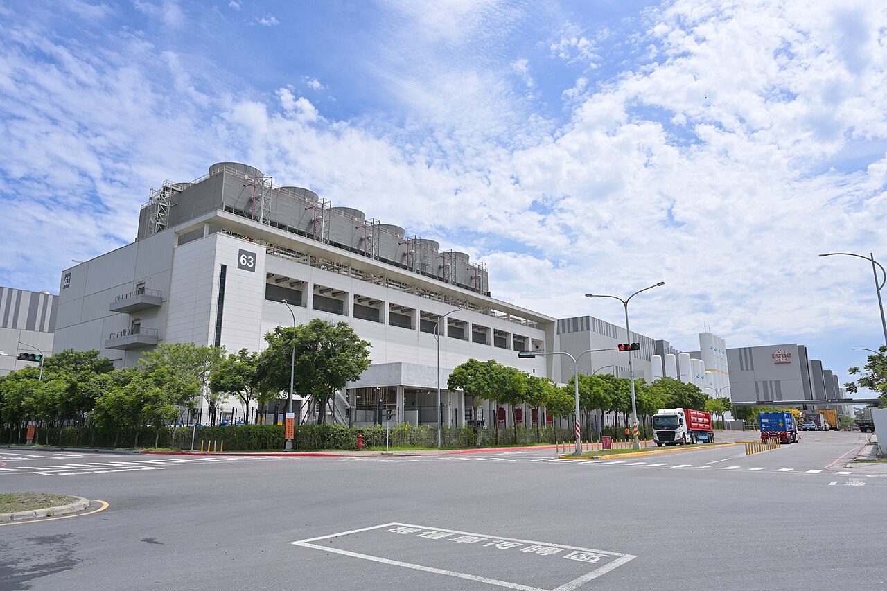
图片来源:图:台积电晶圆厂(资料图)。图片来源:Wikimedia Commons,CC BY 4.0。Photo: A TSMC fabrication plant (file photo). Image: via Wikimedia Commons, CC BY 4.0.
GSM Global · 本篇英文版 English edition of this story