商务部与格芯修订芯片奖励安排:9.55亿美元改投硅光子与先进封装 格芯在美投资扩至50亿美元

华盛顿——美国商务部10月14日宣布,该部芯片计划办公室已与半导体代工企业格芯(GlobalFoundries)达成协议,修订其现有的《芯片与科学法》(CHIPS and Science Act)奖励安排:将最高9.55亿美元激励资金重新定向,用于加速硅光子、硅锗技术与先进封装领域的投资,奖励总额不变。
按修订安排,格芯将把其位于纽约州马耳他(Malta)与佛蒙特州伯灵顿(Burlington)两处工厂的资本投资扩大至50亿美元,扩充硅光子与硅锗产能,并建设美国首个先进封装用硅中介层(silicon interposer)产能,服务于通信基础设施与数据中心需求。
格芯总部位于纽约州马耳他,是美国本土主要的晶圆代工企业之一。商务部表示,此次修订意在把既有奖励集中投向对美国半导体供应链更关键的技术环节。
Commerce Department Reallocates $955 Million of GlobalFoundries CHIPS Award to Silicon Photonics and Advanced Packaging
Washington — The Department of Commerce announced on October 14 that its CHIPS Program Office has reached an agreement with semiconductor foundry GlobalFoundries to amend the company's existing CHIPS and Science Act award, reallocating up to $955 million in incentives to accelerate investments in silicon photonics, silicon-germanium and advanced packaging. The total award amount is unchanged.
Under the amended award, GlobalFoundries will expand its capital investments at its Malta, New York, and Burlington, Vermont, facilities to $5 billion, growing silicon photonics and silicon-germanium capacity and building the first U.S. production capacity for silicon interposers used in advanced packaging, aimed at communications infrastructure and data centers.
GlobalFoundries, headquartered in Malta, New York, is one of the largest U.S.-based wafer foundries. The department said the amendment concentrates the existing award on technology areas it considers most critical to the U.S. semiconductor supply chain.
发布:GSM·美国(发布链接)
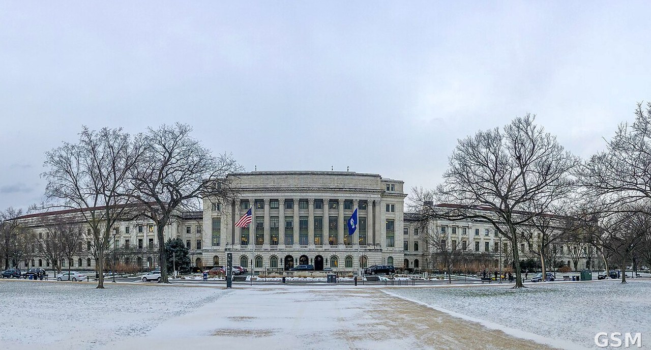
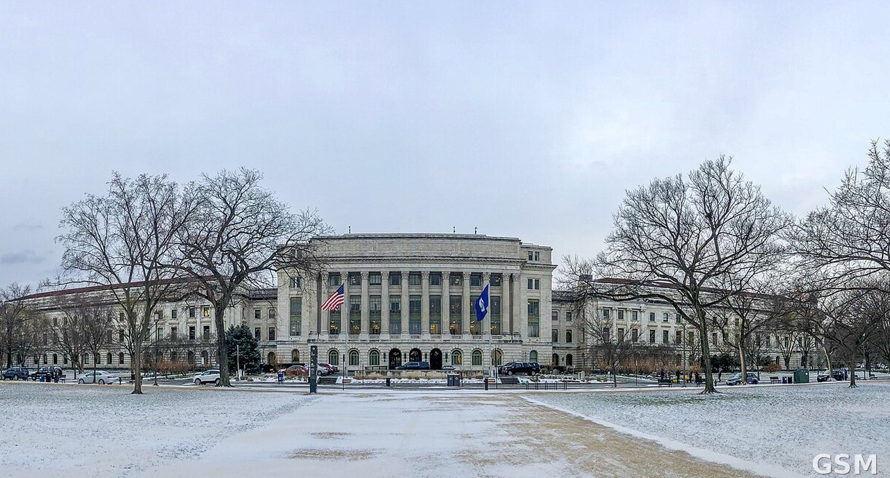
图片来源:图:位于华盛顿特区的美国商务部总部赫伯特·C·胡佛大楼(资料图)。图片来源:Wikimedia Commons,APK 摄,CC BY-SA 4.0 授权 / Photo: The Herbert C. Hoover Building, U.S. Department of Commerce headquarters in Washington, D.C. (file photo). Source: Wikimedia Commons, by APK, CC BY-SA 4.0.
GSM Global · 本篇英文版 English edition of this story