联电与爱普记忆合作 AI 供电方案:S-SiCap Gen2D 硅电容已完成流片与初步验证
联华电子(联电)与爱普记忆 10 月 22 日宣布达成技术与制造合作,共同推进面向人工智能与高性能计算(HPC)系统的供电方案:联电提供深沟槽电容(DTC)代工技术与可扩展的晶圆制造能力,爱普记忆提供硅电容设计与系统级整合,解决下一代数据中心的供电效率问题。
据双方新闻稿,随着 AI 负载快速增长,数据中心供电架构正从把稳压元件放在电路板上,转向把电容器直接嵌入中介层或基板,以缩短供电路径、改善电源完整性。合作已在 2026 年第三季度达到一个重要节点:爱普记忆的 S-SiCap Gen2D 分立式硅电容设计已完成流片与初步功能验证。下一步将对基板封装中的电容进行全面的系统级性能与可靠性测试,并支持不同电容值与工作电压需求。双方还在探索把合作扩展到电容嵌入式中介层与背面(landside)电容等其他产品线。
联电资深副总 GC Hung 表示:「AI 与 HPC 的增长正推动供电方式的根本转变——从电路板级走向芯片级的垂直供电整合。联电提供包括 DTC 技术在内的稳健供电方案,让高密度电容更靠近计算芯片、实现更稳定的供电。与爱普记忆合作,我们正把可扩展的方案推向市场,解决 AI 基础设施持续演进中的关键供电瓶颈。」爱普记忆总裁 Ivan Hong 表示,S-SiCap 定制产品采用 DTC 技术成功流片并完成初步晶圆验证,是展示其设计灵活性与可制造性的重要里程碑;与联电合作可为客户提供从产品设计到晶圆制造的整体方案。
新闻稿还介绍,联电的供电方案路线图涵盖分立式与嵌入式硅电容,并延伸至内部稳压器等主动元件;公司正利用其先进封装能力实现更高密度的电源元件整合,并持续投资新产能。联电在全球设有 12 座晶圆厂,合计月产能超过 40 万片(12 英寸约当量),总部位于台湾新竹,员工约 2 万人。
联电在 GSM《全球芯片公司排名榜》中居第 19 名(2025 年营收约 75 亿美元);在晶圆代工分榜(TrendForce,2026 年第二季度)居全球第 4 名,份额 3.9%。
UMC and AP Memory Team Up on AI Power Delivery; S-SiCap Gen2D Tapes Out on UMC's Deep Trench Capacitor Technology
United Microelectronics Corporation (UMC) and AP Memory announced a technology and manufacturing collaboration on October 22 to advance power delivery solutions for AI and high-performance computing (HPC) systems. The partnership combines UMC's deep trench capacitor (DTC) foundry technology and scalable wafer manufacturing with AP Memory's silicon capacitor designs and system-level integration, addressing the power efficiency challenges of next-generation data centers.
Rapid scaling of AI workloads is driving a shift in data center design from placing power stabilization components on the circuit board to embedding capacitors directly in the interposer or substrate, which shortens the power delivery path and improves power integrity, the companies said. The collaboration reached a milestone in the third quarter of 2026, with AP Memory's S-SiCap Gen2D discrete silicon capacitor designs completing tape-out and initial functional validation. The next step is comprehensive system-level performance and reliability testing of capacitors in substrate packages, and the two companies are also exploring extending the collaboration to capacitor-embedded interposers and landside capacitors.
"The growth of AI and HPC is driving a fundamental shift in power delivery – from board-level towards increasingly vertical power integration on the chip-level," said GC Hung, Senior Vice President of UMC. "By partnering with AP Memory, we are helping to bring scalable solutions to the market to solve the critical power bottleneck challenges as AI infrastructure continues to evolve." Ivan Hong, President of AP Memory, said the successful tape-out and initial wafer validation of customized S-SiCap products using DTC technology demonstrates the flexibility and manufacturability of AP Memory's S-SiCap design, and that working with UMC provides customers a total solution from product design to wafer manufacturing.
UMC said its power delivery roadmap covers both discrete and embedded silicon capacitors and extends to active components such as internal voltage regulators, and that it is investing in new manufacturing capacity for power delivery and heterogeneous integration. UMC operates 12 fabs with combined capacity of more than 400,000 wafers per month (12-inch equivalent), is headquartered in Hsinchu, Taiwan, and employs about 20,000 people worldwide.
UMC ranks No. 19 in GSM's Global Chip Company Rankings, with 2025 revenue of about $7.5 billion, and No. 4 among foundries with a 3.9% share (TrendForce, Q2 2026).
来源:GSM·美国(原文链接)
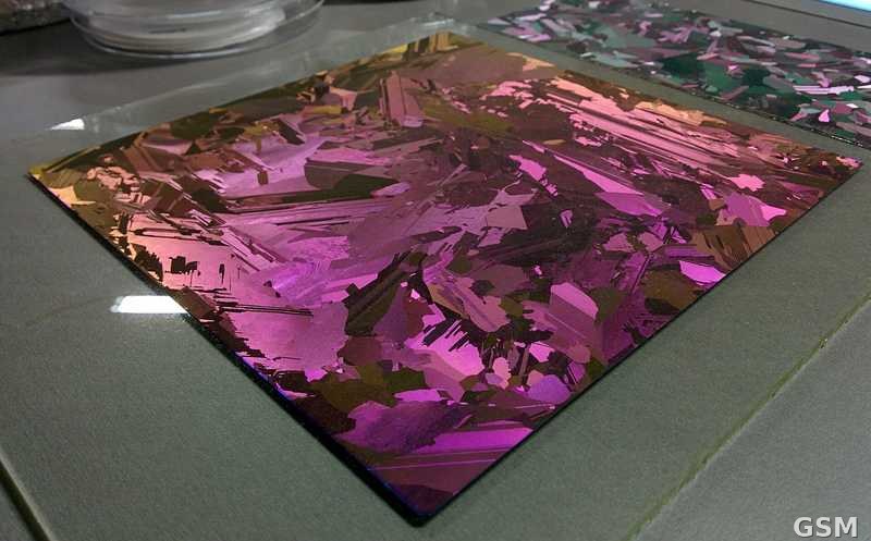
图片来源:图:多晶硅晶圆资料图。照片:Radiotrefoil,CC BY-SA 4.0,经 Wikimedia Commons。Photo: A multicrystalline silicon wafer (file photo). Photo: Radiotrefoil, CC BY-SA 4.0, via Wikimedia Commons.