SK 海力士提出 AI 内存新瓶颈论:3D 堆叠 DRAM 与高带宽闪存进入路线图 HBM4E 样品单引脚 16Gb/s
首尔——SK 海力士总裁兼首席开发官 Ahn Hyun 10 月 14 日在首尔 COEX 开幕的第 28 届半导体展览会(SEDEX 2026)主旨演讲中表示,AI 基础设施的新瓶颈已从计算单元与内存之间,转移到不同内存层级之间的数据移动本身。他提出以 3D 堆叠 DRAM 与高带宽闪存(HBF)密集连接整个内存层级。
3D 堆叠 DRAM 将 DRAM 芯片直接堆叠在 GPU、NPU 等逻辑芯片之上,以硅通孔(TSV)垂直键合,区别于现有经中介层横向交换数据的 2.5D 封装。Ahn Hyun 表示,垂直通路使数据移动距离大幅缩短,输入输出端子数量可达 HBM 的数十倍,带宽最大化的同时显著降低功耗。
HBF 把 HBM 的堆叠工艺移植到 NAND 闪存上:带宽约为同代 HBM 的一半,容量可达 10 倍以上。SK 海力士与闪迪等伙伴推进 HBF 标准化,已通过开放计算项目(OCP)发布 0.7 版规范——最高 512GB 容量、按等级 0.4 至 3.0 TB/s 带宽、采用 UCIe 芯粒接口;公司目标 2027 年初完成最终规范,「HBF Cube」样品计划 2028 年初出货。Ahn Hyun 指出,AI 推理负载中写入操作占比极低,可绕开 NAND 的写入寿命限制,预取技术则用于弥补 NAND 的延迟。
现有产品线方面,SK 海力士 HBM4 已于今年二季度开始量产供货;12 层 HBM4E 样品已于 6 月向主要客户出货,容量 48GB、单引脚数据速率最高 16 Gb/s;公司计划在 HBM4E 与 HBM5 世代提高定制化 HBM 的比重。公司并在推进基于 CXL 的内存池,以及内部架构全面重构、目标输入输出操作(IOPS)达现行水平 4 至 8 倍的「Storage Next」固态硬盘,已与多家大型科技公司完成概念设计。
系统层面,SK 海力士副总裁 Kim Ho-sik 10 月 12 日在圣何塞举行的 OCP 全球峰会上提出「以内存为中心的 AI 机架系统」(MARS):将内存从 CPU 与 GPU 上解耦、汇成大规模内存池按需分配。公司称,在多轮 AI 智能体推理服务的实测中,MARS 把首个词元生成时间(TTFT)较重新计算方案改善 3 至 5 倍。Ahn Hyun 在演讲中预计,按复杂推理、上下文长度与每秒推理请求三项因素叠加,AI 基础设施的性能规模到 2030 年将扩张至 2026 年的约 19 至 20 倍。
SK 海力士在 GSM《全球芯片公司排名榜》(2025 年口径)中居全球第 3 名,HBM 营收份额约 50% 居全球第一(TrendForce,2026 年第二季度)。
SK hynix Flags Data Movement Between Memory Tiers as AI's New Bottleneck; 3D Stacked DRAM and High-Bandwidth Flash Join the Roadmap
SEOUL — The bottleneck in AI infrastructure has shifted from the gap between compute and memory to data movement between memory tiers themselves, SK hynix President and Chief Development Officer Ahn Hyun said in a keynote at the 28th Semiconductor Exhibition (SEDEX 2026), which opened on October 14 at COEX in Seoul. He proposed connecting the entire memory hierarchy densely through 3D stacked DRAM and high-bandwidth flash (HBF).
3D stacked DRAM places DRAM dies directly on top of logic dies such as GPUs and NPUs, bonded vertically through silicon vias — a departure from today's 2.5D packaging, where data moves laterally through an interposer. By shortening the data path, Ahn said, I/O terminals can be increased by tens of times compared with HBM, maximizing bandwidth while sharply cutting power consumption.
HBF transplants HBM's stacking technology onto NAND flash, offering roughly half the bandwidth of same-generation HBM at more than ten times the capacity. SK hynix is driving HBF standardization with partners including SanDisk and has released version 0.7 of the specification through the Open Compute Project: up to 512GB capacity, 0.4 to 3.0 TB/s of bandwidth by grade, and a UCIe chiplet interface. The company targets a final specification in early 2027 and "HBF Cube" samples in early 2028. Ahn noted that writes make up an extremely small share of AI inference workloads, sidestepping NAND's endurance limits, while prefetching addresses its latency.
On current products, SK hynix began volume supply of HBM4 in the second quarter of this year, and its 12-high HBM4E samples shipped to key customers in June offer 48GB capacity at up to 16 Gb/s per pin; the company plans to raise the share of customized HBM across the HBM4E and HBM5 generations. It is also building CXL-based pooled memory and has completed conceptual design with major technology companies for "Storage Next" SSDs that redesign internal architecture for four to eight times today's IOPS.
At the system level, Vice President Kim Ho-sik presented the Memory-Centric AI Rack System (MARS) at the OCP Global Summit in San Jose on October 12: memory is disaggregated from CPUs and GPUs into a large shared pool allocated on demand. In multi-turn AI agent inference tests, SK hynix said, MARS improved time to first token by three to five times versus recomputation approaches. Ahn projected that AI infrastructure performance scale will expand to roughly 19 to 20 times 2026 levels by 2030, driven by complex reasoning, longer contexts and more inference requests per second.
SK hynix ranks No. 3 in GSM's Global Chip Company Rankings on 2025 revenue, and holds about 50% of HBM revenue, the world's largest share (TrendForce, Q2 2026).
来源:GSM·美国(原文链接)
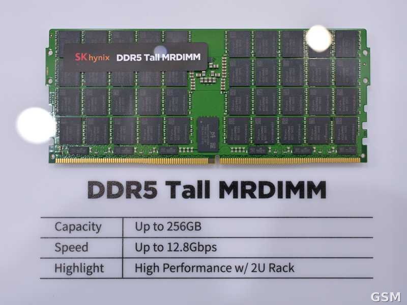
图片来源:图:SK 海力士 DDR5 Tall MRDIMM 内存产品展示。照片:4300streetcar,CC BY 4.0,经 Wikimedia Commons。Photo: SK hynix DDR5 Tall MRDIMM modules on display. Photo: 4300streetcar, CC BY 4.0, via Wikimedia Commons.