美光公布存储路线图:HBM 一年一代排至 2030 年 1δ DRAM 节点 2027 年下半年量产
美光科技在 10 月 21 日举行的技术网络研讨会上系统公布了下一代存储路线图:高带宽存储(HBM)将以每年一代的节奏推进——HBM4 已进入大规模量产、每堆叠带宽 2.8 TB/s,HBM4E 已向主要客户送样,按计划 2027 年 HBM4E 量产、2028 年 HBM5、2029 年 HBM5E、2030 年 HBM6。公司首席技术官 Scott DeBoer 在会上主讲该路线图。
路线图还包括两种新的堆叠形态:vHBM 将 HBM 直接垂直堆叠在计算芯片之上,省去中介层(interposer);面向边缘推理的 vEIM 每堆叠带宽约 2 TB/s、能效优于每比特 1 皮焦。DRAM 制程方面,1δ(1-delta)节点计划 2027 年下半年爬坡量产,位密度较 1γ 节点提升逾两成;该节点将支撑 DDR6(理论带宽为 DDR5 的两倍以上)与 LPDDR6,后者能效较 LPDDR5 提升逾 35%。服务器内存方面,512GB DDR5 RDIMM 已在送样,1TB 容量的 RDIMM 正在开发。
NAND 方面,美光下一代 G11 节点将超过 400 层,位密度约为 G9 的两倍、输入输出速度提升约 1.5 倍、单次数据传输能耗降低逾 25%,采用晶圆对晶圆键合技术,计划 2027 年下半年爬坡。谈及业界讨论的 4F² 单元架构,DeBoer 在接受日经亚洲采访时表示,该架构不在美光的路线图上,其密度优势「多少是个神话」。
美光在 GSM《全球芯片公司排名榜》(2025 年口径)中居全球第 5 名,2025 年营收 415 亿美元、同比增长 50.2%;按 TrendForce 2026 年第二季度数据,美光 DRAM 营收份额 23.3% 居第 3 名,HBM 营收份额约 18%。
Micron Unveils Memory Roadmap: A New HBM Generation Every Year Through 2030; 1δ Node to Ramp in Late 2027
Micron Technology laid out its next-generation memory roadmap at a technology webinar on October 21: high-bandwidth memory will advance one generation per year — HBM4 is already in high-volume production at 2.8 TB/s per stack, HBM4E is sampling to key customers, and the company targets HBM4E in volume in 2027, followed by HBM5 in 2028, HBM5E in 2029 and HBM6 in 2030. Chief Technology Officer Scott DeBoer presented the roadmap at the event.
The roadmap also includes vHBM, a new stacking approach that places HBM vertically on top of the compute die and eliminates the interposer, and vEIM, an edge-inference design targeting about 2 TB/s per stack at under 1 picojoule per bit. On the DRAM process side, the 1δ (1-delta) node is slated to ramp in the second half of 2027 with bit density more than 20% above the 1γ node; it will underpin DDR6, with more than twice the theoretical bandwidth of DDR5, and LPDDR6, with power efficiency more than 35% better than LPDDR5. For server memory, 512GB DDR5 RDIMMs are sampling and a 1TB RDIMM is in development.
On NAND, Micron's next G11 node will exceed 400 layers, with roughly twice the bit density of G9, about 1.5 times the I/O speed and more than 25% less energy per data transfer, using wafer-to-wafer bonding, with a ramp planned for the second half of 2027. Asked about the 4F² cell architecture discussed in the industry, DeBoer told Nikkei Asia that it is not on Micron's roadmap and that its density advantage is "a bit of a myth."
Micron ranks No. 5 in GSM's Global Chip Company Rankings on 2025 revenue of $41.5 billion, up 50.2%. In Q2 2026 TrendForce data, Micron held a 23.3% share of DRAM revenue, third globally, and about 18% of HBM revenue.
来源:GSM·美国(原文链接)
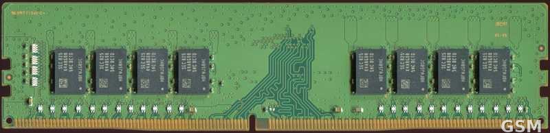
图片来源:图:DDR4 内存条(DRAM 存储芯片)资料图。照片:PantheraLeo1359531,CC BY 4.0,经 Wikimedia Commons。Photo: A DDR4 memory module (file photo). Photo: PantheraLeo1359531, CC BY 4.0, via Wikimedia Commons.